- 您现在的位置:买卖IC网 > Sheet目录3890 > PIC16C717T-E/SS (Microchip Technology)IC MCU OTP 2KX14 A/D PWM 20SSOP
PIC16C717/770/771
DS41120B-page 116
2002 Microchip Technology Inc.
11.10 A/D Operation During SLEEP
The A/D module can operate during SLEEP mode. This
requires that the A/D clock source be configured for RC
(ADCS<1:0> = 11b). With the RC clock source
selected, when the GO/DONE bit is set the A/D module
waits one instruction cycle before starting the conver-
sion cycle. This allows the SLEEP instruction to be exe-
cuted, which eliminates all digital switching noise
during the sample and conversion. When the conver-
sion cycle is completed the GO/DONE bit is cleared,
and the result loaded into the ADRESH and ADRESL
registers. If the A/D interrupt is enabled, the device will
wake-up from SLEEP. If the A/D interrupt is not
enabled, the A/D module will then be turned off,
although the ADON bit will remain set.
When the A/D clock source is another clock option (not
RC), a SLEEP instruction causes the present conver-
sion to be aborted and the A/D module is turned off,
though the ADON bit will remain set.
Turning off the A/D places the A/D module in its lowest
current consumption state.
11.11 Connection Considerations
Since the analog inputs employ ESD protection, they
have diodes to VDD and VSS. This requires that the
analog input must be between VDD and VSS. If the input
voltage exceeds this range by greater than 0.3V (either
direction), one of the diodes becomes forward biased
and it may damage the device if the input current spec-
ification is exceeded.
An external RC filter is sometimes added for anti-alias-
ing of the input signal. The R component should be
selected to ensure that the total source impedance is
kept under the 2.5 k
recommended specification. It is
recommended that any external components con-
nected to an analog input pin (capacitor, zener diode,
etc.) have very little leakage current.
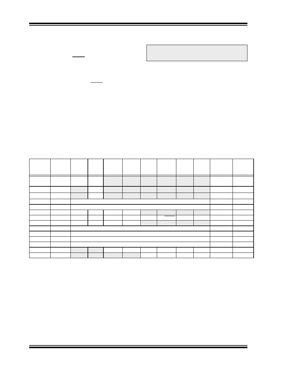
TABLE 11-2:
SUMMARY OF A/D REGISTERS
Note:
For the A/D module to operate in SLEEP,
the A/D clock source must be configured to
RC (ADCS<1:0> = 11).
Address
Name
Bit 7
Bit 6
Bit 5
Bit 4
Bit 3
Bit 2
Bit 1
Bit 0
Value on:
POR,
BOR
Value on
all other
RESETS
0Bh,8Bh,
10Bh,18Bh
INTCON
GIE
PEIE
T0IE
INTE
RBIE
T0IF
INTF
RBIF
0000 000x
0000 000u
0Ch
PIR1
—
ADIF
—
SSPIF
CCP1IF
TMR2IF
TMR1IF
-0-- 0000
8Ch
PIE1
—
ADIE
—
SSPIE
CCP1IE
TMR2IE
TMR1IE
-0-- 0000
1Eh
ADRESH
A/D High Byte Result Register
xxxx xxxx
uuuu uuuu
9Eh
ADRESL
A/D Low Byte Result Register
xxxx xxxx
uuuu uuuu
9Bh
REFCON
VRHEN
VRLEN
VRHOEN
VRLOEN
—
0000 ----
1Fh
ADCON0
ADCS1
ADCS0
CHS2
CHS1
CHS0
GO/DONE
CHS3
ADON
0000 0000
9Fh
ADCON1
ADFM
VCFG2
VCFG1
VCFG0
—
0000 ----
05h
PORTA
PORTA Data Latch when written: PORTA pins when read
000x 0000
000u 0000
06h
PORTB
PORTB Data Latch when written: PORTB pins when read
xxxx xx11
uuuu uu11
85h
TRISA
PORTA Data Direction Register
1111 1111
86h
TRISB
PORTB Data Direction Register
1111 1111
9Dh
ANSEL
—
ANS5
ANS4
ANS3
ANS2
ANS1
ANS0
1111 1111
17h
CCP1CON
—
0000 0000
Legend: x = unknown, u = unchanged, - = unimplemented read as ’0’. Shaded cells are not used for A/D conversion.
发布紧急采购,3分钟左右您将得到回复。
相关PDF资料
PIC16LC770T-E/SO
IC MCU OTP 2KX14 A/D PWM 20SOIC
PIC16C771T/SO
IC MCU OTP 4KX14 A/D PWM 20SOIC
PIC16LC717T-I/SS
IC MCU OTP 2KX14 A/D PWM 20SSOP
PIC16C717T/SS
IC MCU OTP 2KX14 A/D PWM 20SSOP
PIC16LC770T-I/SO
IC MCU OTP 2KX14 A/D PWM 20SOIC
PIC16LC771T-E/SS
IC MCU OTP 4KX14 A/D PWM 20SSOP
PIC16C771T-E/SS
IC MCU OTP 4KX14 A/D PWM 20SSOP
PIC16LC771T-I/SO
IC MCU OTP 4KX14 A/D PWM 20SOIC
相关代理商/技术参数
PIC16C717T-I/SO
功能描述:8位微控制器 -MCU 3.5KB 256 RAM 16 I/O RoHS:否 制造商:Silicon Labs 核心:8051 处理器系列:C8051F39x 数据总线宽度:8 bit 最大时钟频率:50 MHz 程序存储器大小:16 KB 数据 RAM 大小:1 KB 片上 ADC:Yes 工作电源电压:1.8 V to 3.6 V 工作温度范围:- 40 C to + 105 C 封装 / 箱体:QFN-20 安装风格:SMD/SMT
PIC16C717T-I/SS
功能描述:8位微控制器 -MCU 3.5KB 256 RAM 16 I/O RoHS:否 制造商:Silicon Labs 核心:8051 处理器系列:C8051F39x 数据总线宽度:8 bit 最大时钟频率:50 MHz 程序存储器大小:16 KB 数据 RAM 大小:1 KB 片上 ADC:Yes 工作电源电压:1.8 V to 3.6 V 工作温度范围:- 40 C to + 105 C 封装 / 箱体:QFN-20 安装风格:SMD/SMT
PIC16C71T-04/SO
功能描述:8位微控制器 -MCU 1.75KB 36 RAM 13 I/O 4MHz SOIC18 RoHS:否 制造商:Silicon Labs 核心:8051 处理器系列:C8051F39x 数据总线宽度:8 bit 最大时钟频率:50 MHz 程序存储器大小:16 KB 数据 RAM 大小:1 KB 片上 ADC:Yes 工作电源电压:1.8 V to 3.6 V 工作温度范围:- 40 C to + 105 C 封装 / 箱体:QFN-20 安装风格:SMD/SMT
PIC16C71T-04I/SO
功能描述:8位微控制器 -MCU 1.75KB 36 RAM 13 I/O 4MHz Ind Temp SOIC18 RoHS:否 制造商:Silicon Labs 核心:8051 处理器系列:C8051F39x 数据总线宽度:8 bit 最大时钟频率:50 MHz 程序存储器大小:16 KB 数据 RAM 大小:1 KB 片上 ADC:Yes 工作电源电压:1.8 V to 3.6 V 工作温度范围:- 40 C to + 105 C 封装 / 箱体:QFN-20 安装风格:SMD/SMT
PIC16C71T-20/SO
功能描述:8位微控制器 -MCU 1.75KB 36 RAM 13 I/O RoHS:否 制造商:Silicon Labs 核心:8051 处理器系列:C8051F39x 数据总线宽度:8 bit 最大时钟频率:50 MHz 程序存储器大小:16 KB 数据 RAM 大小:1 KB 片上 ADC:Yes 工作电源电压:1.8 V to 3.6 V 工作温度范围:- 40 C to + 105 C 封装 / 箱体:QFN-20 安装风格:SMD/SMT
PIC16C71T-20I/SO
功能描述:8位微控制器 -MCU 1.75KB 36 RAM 13 I/O RoHS:否 制造商:Silicon Labs 核心:8051 处理器系列:C8051F39x 数据总线宽度:8 bit 最大时钟频率:50 MHz 程序存储器大小:16 KB 数据 RAM 大小:1 KB 片上 ADC:Yes 工作电源电压:1.8 V to 3.6 V 工作温度范围:- 40 C to + 105 C 封装 / 箱体:QFN-20 安装风格:SMD/SMT
PIC16C72/JW
功能描述:8位微控制器 -MCU 3.5KB 128 RAM 22 I/O RoHS:否 制造商:Silicon Labs 核心:8051 处理器系列:C8051F39x 数据总线宽度:8 bit 最大时钟频率:50 MHz 程序存储器大小:16 KB 数据 RAM 大小:1 KB 片上 ADC:Yes 工作电源电压:1.8 V to 3.6 V 工作温度范围:- 40 C to + 105 C 封装 / 箱体:QFN-20 安装风格:SMD/SMT
PIC16C72-04/SO
功能描述:8位微控制器 -MCU 3.5KB 128 RAM 22 I/O RoHS:否 制造商:Silicon Labs 核心:8051 处理器系列:C8051F39x 数据总线宽度:8 bit 最大时钟频率:50 MHz 程序存储器大小:16 KB 数据 RAM 大小:1 KB 片上 ADC:Yes 工作电源电压:1.8 V to 3.6 V 工作温度范围:- 40 C to + 105 C 封装 / 箱体:QFN-20 安装风格:SMD/SMT